mini Workshop


Be part of our mini-Workshop scheduled for
 

October 30th, 2023

3 PM – 5 PM
(CET)

 
and join online here


Penghan Lu
FZ Jülich, Germany

Welcome and introduction

Invited Talk
4D STEM-in-SEM: Fleeting Fancy or Foundation for the Future?

The recent emergence of 4D STEM has garnered much attention in the electron microscopy community, and with good reason. The amount of information
available in a 4D dataset, and the number of ways to extract or glean different information for diverse applications is almost limitless. Although much of the new interest and development has occurred in the high-kV S/TEM realm, the concept of collecting a diffraction pattern at every beam raster position is routine in the SEM community. One only needs to consider EBSD (conventional or transmission), to realize that a solid foundation for 4D STEM-in-SEM has already been established.
The first part of this talk will provide a brief description of STEM-in-SEM activities at NIST-Boulder, with emphasis on 4D STEM-in-SEM. Current work
on software, hardware, and their application to different material systems will be presented, with an overarching goal of showing that low-kV electron diffraction can provide information on par with that obtained in a TEM or by X-ray diffraction. In addition to the usual 4D STEM approach to collecting data, we show different ways to use the equipment to collect useful diffraction information without resorting to collecting a complete 4D dataset. The second part of this talk will be dedicated to outlining some of the opportunities and hurdles inherent to low-kV transmission electron microscopy in a conventional SEM (i.e., instrumentation, hardware and software advancement needs, technology transfer, standards development, best practices, diffraction pattern interpretation anxiety, beam damage and adventitious carbon, cost, AI/ML opportunities, M-C scattering simulations enhanced with diffraction capabilities, etc.). The intent here is to stimulate ideas for discussion and to offer different opportunities for the SEM community to build on an already solid platform.

Johannes Müller
HU Berlin, Germany

Invited Talk
4D STEM-in-SEM at HU Berlin: Our instrumentation and application examples

4D STEM is a diffraction-based technique and allows to map material properties like layer thickness, crystal orientations, crystallite size, crystallinity, and many more properties. 4D STEM can also be employed in conventional scanning electron microscopes (SEMs) to investigate thin bulk and low-dimensional
materials by inserting a fast camera below the electron-transparent sample. We will present our in-house developed instrumentation and show a summary of our implemented methods and applications.

Dr. Subin Lee
KIT, Germany

Invited Talk
Developing 4D STEM-in-SEM with direct electron detector

Four-dimensional scanning transmission electron microscopy (4D STEM) has opened new avenues in nanoscale material characterization, offering insights into microstructure and phase information. Advancements now extend this technique to scanning electron microscopy (SEM), expanding its reach beyond TEM. While 4D STEM-in-SEM has been utilized for 2D materials, its potential remains unexplored in bulk metallic materials like aluminum alloys, superalloys, and metallic thin films. Challenges in sample preparation and SEM parameters exist, but using a MiniPix TPX3 detector, we captured 10,000 diffraction patterns across 100×100 SEM pixels in just eight seconds, showcasing the rapid data acquisition for real-time studies which open possibilities to record dynamic phenomena such as phase transformations and chemical reactions in real space. Virtual BF and DF images can be developed, which helps determine the crystal structures and local strains. The talk also encompasses the challenges of sample preparation and microscope parameters for a successful run of 4D STEM-in-SEM.

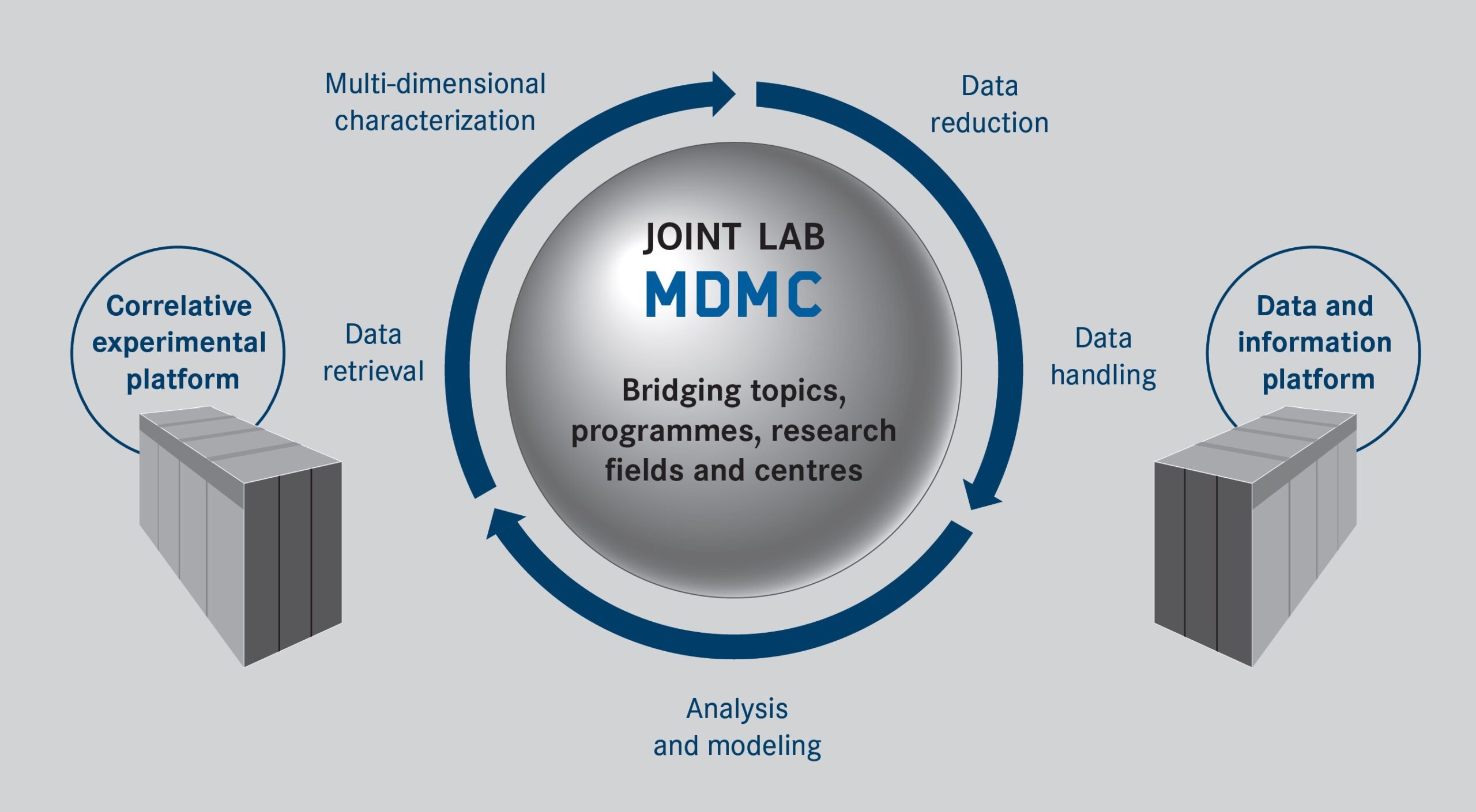
The Joint Lab Model Driven Materials Characterization is a cross-centre platform of the Helmholtz Association.